


Since the humble beginning in 1988, Waddan has advanced the state of the art in a number of technologies. It has been doing micro-machining before the term MEMS was coined. For packaging its devices for consumer use, it has developed fabrication methods for high resolution PCBs, smaller systems, embedded systems, small footprint firmware, innovative electronic design, and built several customized test stations. Not only these technologies and hardware are for in-house applications, but are available to outside users as a service.
The list of services provided to the customers is listed on the right. The company also provides other related Design and Simulation sevices:
Finding help for processing wafers in an evolutionary technology area
is difficult and time consuming. Waddan's vertical processing structure
avoids fab hopping if you are new in the field or if you want to stay
fab-less. Waddan can prepare masks based on your device design to
process devices at Waddan Systems, or supply professional quality masks
for intermediate or post-processing for external work.
Although Waddan's expertise allows for practically any 3-D structure to
be built in crystalline materials, it will not impose its solutions and
designs unless consulted upon. It will simply provide information on
what is currently available as far as mask making goes at Waddan
Systems. Nevertheless, all customer confidential data is handled and
archived or destroyed as per mutual agreement.
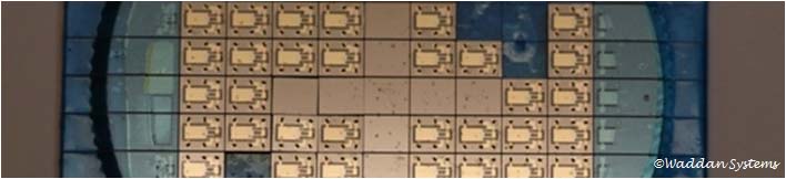
Once the device baseline design is completed, it goes through several
iterations based upon wafer fab involved. Every wafer fab has its own
idiosyncrasy, even when identical equipments are employed. The next
step, after design verification, is process design and the order of
processing steps. Each processing step may require one or more image
patterning sub-steps. The pattern-generation uses photolithography, and
that requires photolithography masks. (No two fabs can exactly
duplicate the same results even when the same masks are used).
Waddan Systems has extensive experience and understands the factors
that influence mask-to-mask registration. It can provide helpful
support during the early stages of development of a product.
