


 Just as a machinist uses machine tools like
lathe, borer, or shaper to
remove material from a block of metal to produce a desired part, a bulk
micromachinist does the same at micro level, only his tools involves
photo processing and chemical etching and some tricks of the .trade
routinely performed in semiconductor industry. A variety of materials
are employed for such micromachining, but silicon is predominantly used
because it is well understood, it is cheaper than other materials in
the processing category, and most importantly the equipment used in
semiconductor industry can be readily customized for this purpose.
Finally, when supporting electronics is necessary, it can be built
around the machined part. In addition to silicon, alumina, sapphire,
Pyrex, quartz, GaAs, Lithium Niobate, Lithium Tantalate etc. are also
employed for sensor manufacturing. With careful design and processing
plans practically any shape imagined
can be formed by bulk micromachining. Nevertheless, to date silicon has
the best processing time and cost advantage over the other materials.
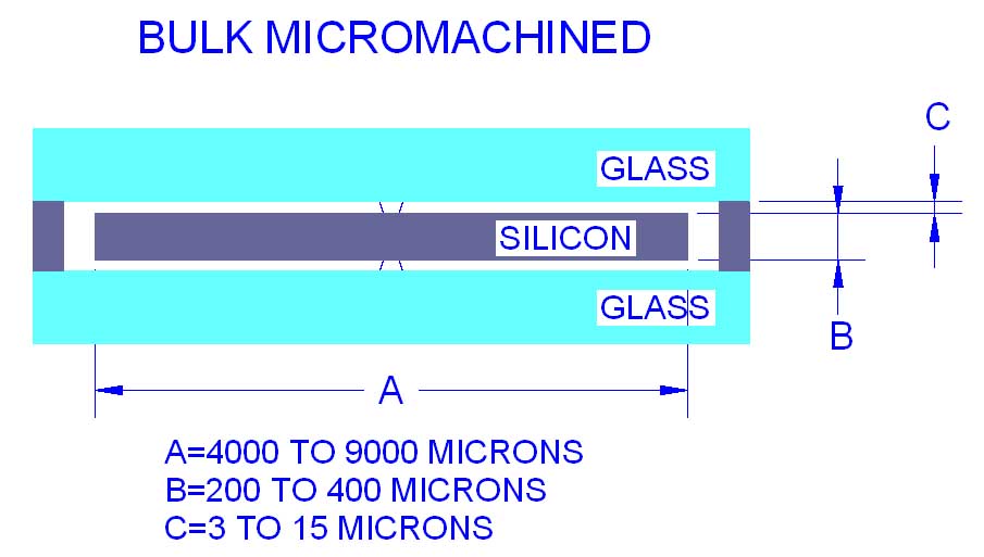
The bulk micromachined devices are usually encapsulated by glass or
some other substrate. Therefore, the devices generally have three
substrates. The typical thicknesses involved are shown in the figure.
Just as a machinist uses machine tools like
lathe, borer, or shaper to
remove material from a block of metal to produce a desired part, a bulk
micromachinist does the same at micro level, only his tools involves
photo processing and chemical etching and some tricks of the .trade
routinely performed in semiconductor industry. A variety of materials
are employed for such micromachining, but silicon is predominantly used
because it is well understood, it is cheaper than other materials in
the processing category, and most importantly the equipment used in
semiconductor industry can be readily customized for this purpose.
Finally, when supporting electronics is necessary, it can be built
around the machined part. In addition to silicon, alumina, sapphire,
Pyrex, quartz, GaAs, Lithium Niobate, Lithium Tantalate etc. are also
employed for sensor manufacturing. With careful design and processing
plans practically any shape imagined
can be formed by bulk micromachining. Nevertheless, to date silicon has
the best processing time and cost advantage over the other materials.
The bulk micromachined devices are usually encapsulated by glass or
some other substrate. Therefore, the devices generally have three
substrates. The typical thicknesses involved are shown in the figure.
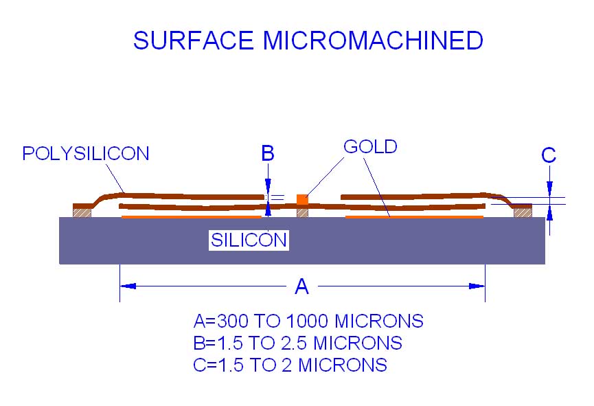 Surface micromachining is the fabrication of
micromechanical structures
by deposition and etching of thick structural and sacrificial films.
Thus, simple microstructures like beams or membranes as well as complex
structures like serpentine springs, gimbals, resonators, switches can
be fabricated on top of a silicon substrate. The main features of the
surface micromachining technology are the small microstructure
dimensions and the opportunity to integrate micromechanics and
microelectronics on the same chip. By use of VLSI compatible batch
processing, low cost microstructure fabrication can be achieved for
high volume applications. However, the thermal warping or distortion of
the sensing element and the flexures involved is a common problem as
the operating temperature varies. Operation at nominally fixed
temperature is necessary for predictable responses.
Surface micromachining is the fabrication of
micromechanical structures
by deposition and etching of thick structural and sacrificial films.
Thus, simple microstructures like beams or membranes as well as complex
structures like serpentine springs, gimbals, resonators, switches can
be fabricated on top of a silicon substrate. The main features of the
surface micromachining technology are the small microstructure
dimensions and the opportunity to integrate micromechanics and
microelectronics on the same chip. By use of VLSI compatible batch
processing, low cost microstructure fabrication can be achieved for
high volume applications. However, the thermal warping or distortion of
the sensing element and the flexures involved is a common problem as
the operating temperature varies. Operation at nominally fixed
temperature is necessary for predictable responses.
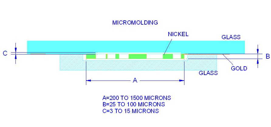 Micromolding is a process of making
electrodeposited castings in molds made in photosensitive sacrificial
materials like PMM resists using optical imaging. Generally, the casts
are 2D structure, but sometimes 3D structures are also made using a
multi-step micromolding technique. The deposition materials chosen are
usually nickel, gold or copper. The molding cavities are made on a
silicon substrate with a Ti film using photolithography. After
completing the deposition, the resist is dissolved leaving the sensing
element along with the surrounding support structures. To complete the
device fabrication, the micromolded elements are transfer bonded to a
Pyrex glass wafer, and the wafer used during deposition is removed by
removing the Ti film.
Micromolding is a process of making
electrodeposited castings in molds made in photosensitive sacrificial
materials like PMM resists using optical imaging. Generally, the casts
are 2D structure, but sometimes 3D structures are also made using a
multi-step micromolding technique. The deposition materials chosen are
usually nickel, gold or copper. The molding cavities are made on a
silicon substrate with a Ti film using photolithography. After
completing the deposition, the resist is dissolved leaving the sensing
element along with the surrounding support structures. To complete the
device fabrication, the micromolded elements are transfer bonded to a
Pyrex glass wafer, and the wafer used during deposition is removed by
removing the Ti film.
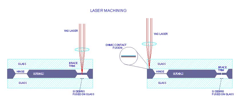 Laser machining is used
mostly for cutting to release sensing elements which otherwise would
break off during wafer processing. In its low power form, the laser is
also used to make positive ohmic contact (welding of two metallic film
surfaces bearing against each other). At microscopic level, a laser cut
line is not as smooth as that made by etching along crystal planes.
That's why it is difficult to form a complete micro device using laser
machining alone. It is mostly used as an assisting technology to trim
parts of structure that is difficult to form using standard methods.
Laser machining is used
mostly for cutting to release sensing elements which otherwise would
break off during wafer processing. In its low power form, the laser is
also used to make positive ohmic contact (welding of two metallic film
surfaces bearing against each other). At microscopic level, a laser cut
line is not as smooth as that made by etching along crystal planes.
That's why it is difficult to form a complete micro device using laser
machining alone. It is mostly used as an assisting technology to trim
parts of structure that is difficult to form using standard methods.
