


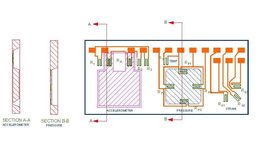
The photo masks are essentially optical fabrication tools for the device. First the design drawing package for the device is prepared. This is available in the form of a 3D solid model or a conventional Plan, Front View and Side View drawings in true scale. Based upon prior wafer processing experience, a sequence of masking steps are designed so that one or more raw wafer substrates can be micromachined to yield the designed device. This iterative process reduces the masking steps into a number of overlapping masking layers, each modifying the substrate incrementally in desired locations. Often the wafers are processed from both sides, and hence, a front-to-back pattern alignment has to be done. This alignment has to be nearly perfect (within 1 micron near the outer edges of the wafer). When multiple substrates are bonded together, the facing wafer-to-wafer alignment is also very critical. A device can have as many as ten masking layers for single sided processing, or twice as many for double sided processing. For example, the ANDAS integrated sensor design shown in the figure above required 12 masking layers.
Once the key parameters of the masking layer are determined, the mask artwork data file is generated. Each mask has a unique ID, which may include a device name, mask layer number, production date, or some other helpful information for the operator (e.g. RIGHT READING FACE DOWN) printed outside the pattern area along the edge of the mask. Other data required for the mask includes:

If the mask art work is constructed in true scale dimensions, any dimensional error made in the artwork gets transferred to the mask in the same scale, i.e. 1 micron error in the artwork shows up as 1 micron error. To make the masks more accurate, the artwork is generally prepared in 10X or 100X scale; and is optically reduced to 1/10 or 1/100 scale on the mask. This reduces any error made in the artwork by the same factor on the mask, i.e. 1 micron error in the artwork reduces to 0.1 or 0.01 micron on the mask. Thus, the mask layer artwork can take the form of :
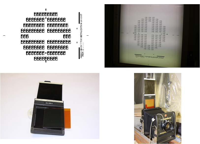
Next, the artwork as prepared above is back illuminated with proper wavelength light:
The set-up shown has been designed to produce a 1/10 inverted image of the transparency layout. A special lens is used that provides uniform reduction of the illuminated object devices from the edges and corners to the center of the layout. The large format film cassettes have been modified to accept mask blanks with photoresist side facing the lens. For best reproduction, the focus, exposure time, aperture and f-stops are pre-determined using trial 4”X5” films. These camera settings are also influenced by the type of photoresist (and its softbake time) applied on the mask blank.
The process of loading the mask blank into the film holder, its insertion behind the camera bellows, and the exposure are all performed in safelite conditions.
Depending upon the photoresist coated on the mask plate blank, a suitable developer is used to develop the mask. If a positive photoresist is involved; wherever it is exposed to UV light it gets dissolved by the developer. Only the photoresist in unexposed regions is left revealing the metal coated on the mask blank. This remaining photoresist serves as a protective cover for the metal underneath it. The mask is cleaned and dried. For protective handling, the photoresist is hardbaked.
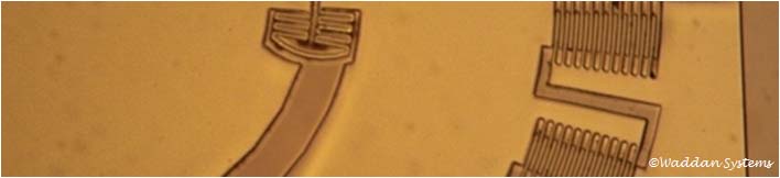
In this step, the mask with hardbaked photoresist pattern (with the exposed through metal) is placed in a chemical bath appropriate for etching the metal. Careful processing controls are exercised to make sure that the metal is neither under etched (making the clear glass pattern translucent or making the clear openings narrower than the design) nor over etched (undercutting the photoresist boundaries or making the clear region dimensions wider than the design). After the metal is etched, the clear glass pattern of the mask appears which can be seen by shining light through.
Up to this point, the mask still has the protective photoresist saving the opaque regions of the mask. The mask is placed in a bath of chemical that completely dissolves this protective photoresist. Slight agitation and bubbling air separates the photoresist from the mask plate. Next, the mask is thoroughly cleaned and dried with nitrogen.
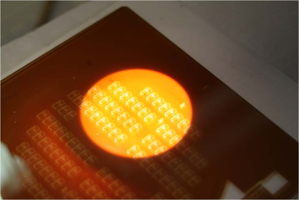
Finally, the mask is visually inspected against the shining light for obvious major defects and flaws. For submicron level anomalies, a high quality microscope with x-y stage micrometers is employed to inspect the mask. The etching pattern is inspected for under or over etching, smoothness of the pattern edges. The actual dimensions of the mask patterns are measured and verified.
For a brief slide show, click on Photomask Production.
