


Just as a machinist uses machine tools like lathe, borer, or shaper to remove material from a block of metal to produce a desired part, a bulk micromachinist does the same at micro level, only his tools involves photo processing and chemical etching and some tricks of the .trade routinely performed in semiconductor industry. A variety of materials are employed for such micromachining, but silicon is predominantly used because it is well understood, it is cheaper other materials in the processing category, and most importantly the equipment used in semiconductor industry can be readily customized for this purpose. Finally, when supporting electronics is necessary, it can be built around the machined part. In addition to silicon, Waddan Systems uses alumina, sapphire, Pyrex, quartz, GaAs, Lithium Niobate, Lithium Tantalate etc. are employed for sensor manufacturing. With careful design and processing plans practically any shape imagined can be formed by bulk micromachining. Nevertheless, to date silicon has the best processing time and cost advantage over the other materials.
Silicon can be etched by isotropic etch and anisotropic etching methods. The isotropic etch as the name indicates moves at nearly the same etching rate along all directions into the material. The anisotropic etch moves at different rates along different crystallographic planes of silicon's cubic structure. One can further control, the rate in a given direction by varying the chemical concentration, composition and temperature of the etchant. There are other factors that influence the etching rates, e.g. how quickly the reacted etchant is removed and fresh etched is brought to the exposed surface. This specially critical when one deals with narrow channels with very high aspect ratios (1:20 to 1:50). Even the surface flow rate and surface tension of the etchant play an important role. The rate differences for 50% KOH at 40 deg C as follows:
When SiO2 is used as mask, it also gets attacked by KOH, but
at a rate about 10% of that of <111> in silicon. The
thickness of the wafer plays a significant role in device designs
requiring etch through etch through if the exposed window in the oxide
is narrower (less than 87% of the wafer thickness for single sided etch
or less than 43.5% of the wafer thickness for double sided back to back
etch), it produces a self limiting V-groove.
Note: Such V-grooves can be made as tapered V-grooves, and very handy
for aligning optical fibers. The V-grooves made for PFOG can be seen in
the MIOC.
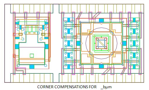
The higher etch rates along <112> and <110>
directions causes an erosion problem at outside corner locations. If
the device design does not have corner compensation, these higher rates
can remove a significant portion of the structure . Some examples of
corner compensation can be seen in square Axlgyro design
 On the other hand the etching rate along
<111>
is not zero, but very small. It causes slight under cutting below the
oxide mask. Waddan Systems exploits this for slowing the etching rate
along <100>. By making a series of very narrow opaque
rectangular strips or diamonds in such a way that the corner erosion
completely undercuts them within a set etch duration and oxide mask
falls off. The sharp edge (for strips) or the pyramid shape (for
diamonds) is left. The sharp structure on top of these shapes expose
new (112) planes and start etching at rates more than two times of that
of <100>. This technique of slowing the etch rate is used
for making braces for device structures that have to be kept in place
during wafer processing. After the anodic bonding with Pyrex on top and
bottom, these braces are
laser trimmed
to isolate these structures from
the neighboring structures either electrically, or mechanically or
both.
On the other hand the etching rate along
<111>
is not zero, but very small. It causes slight under cutting below the
oxide mask. Waddan Systems exploits this for slowing the etching rate
along <100>. By making a series of very narrow opaque
rectangular strips or diamonds in such a way that the corner erosion
completely undercuts them within a set etch duration and oxide mask
falls off. The sharp edge (for strips) or the pyramid shape (for
diamonds) is left. The sharp structure on top of these shapes expose
new (112) planes and start etching at rates more than two times of that
of <100>. This technique of slowing the etch rate is used
for making braces for device structures that have to be kept in place
during wafer processing. After the anodic bonding with Pyrex on top and
bottom, these braces are
laser trimmed
to isolate these structures from
the neighboring structures either electrically, or mechanically or
both.
Waddan Systems also employs deep-trench lithography for making patterns
on surfaces that are not in contact with glass mask during wafer
alignment. Although, the braces can be made by deep-trench
lithography, it is avoided because each lithography on (111) plane
leaves a step, and imaginging across this step with puddled photoresist
requires multiple exposure and development sequence.
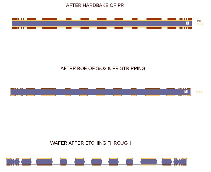
Generally, the depth of etch is controlled by time involved in etching.
Waddan Systems routinely controls the depth tolerance within +/-30 nm.
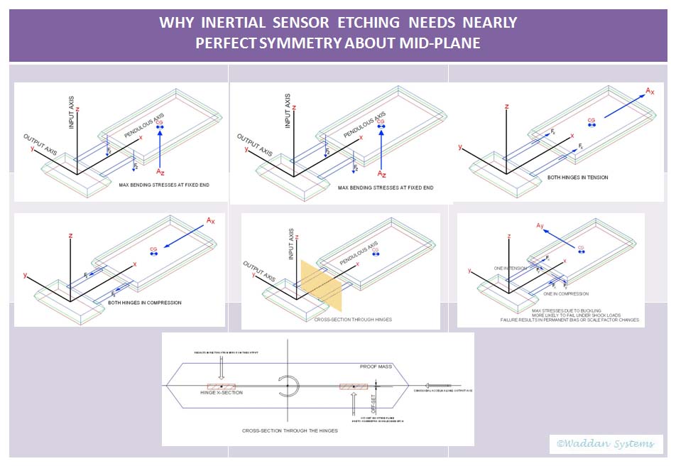
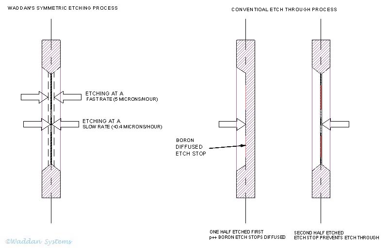
When double sided wafers are employed for making diaphragm like
structures close to one face of the wafer, p++ diffusion etch stops are
used. However, this method is unsuited for making symmetric devices
(such as inertial sensors) about the mid-plane. Usually cantilever
beams are used as hinges in accelerometers, and gimbals are used for
gyros. The cross-section of the structures is about 5 microns in
thickness and 25 microns in width. The offset between the centroid of
the sectional area of these suspension structures and the wafer mid
plane needs to be less than 5nm. The p++ diffusion etch stopping
approach cannot yield such fine tolerance. A double simultaneous
etching approach was developed.
Common chemicals used in anisotropic etching processes are:
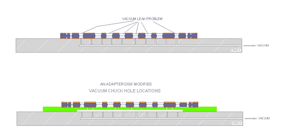
The wafers used for these sensors are double sided polished wafers with their flat planes parallel to each other within 2 microns or less. The optimal thickness of a starting wafer is 250 microns. If the wafer is too thick, it may not etch through due to self limiting V-grooves, or the devices would be too large. If the wafer is too thin, during processing after etch through, it may crack along crystal planes. To minimize such cracking, the edges of the wafers are rounded. The accuracy requirements of the inertial sensors dictate that they should almost perfectly symmetric about the mid-plane of the wafers as illustrated in the following diagrams.
 Navigation
grade sensors has to be insensitive to any inputs in a plane
perpendicular to their input axis. This is only possible when there is
no off-set between the centroid of the inertial mass and the center of
device suspension as illustrated in the above
diagrams. Use of p++ ecth
stops does not yield the symmetry required.
Navigation
grade sensors has to be insensitive to any inputs in a plane
perpendicular to their input axis. This is only possible when there is
no off-set between the centroid of the inertial mass and the center of
device suspension as illustrated in the above
diagrams. Use of p++ ecth
stops does not yield the symmetry required.
This requirement of symmetry leads to symmetrical processing
requirement. The wafers have to be machined simultaneously under the
same conditions from both sides. That requires that they be aligned
from both sides at they same time. This is achieved by growing thermal
oxide (0.5 micron thick) on the wafer surfaces and using a thin
photoresist to coat the wafers:
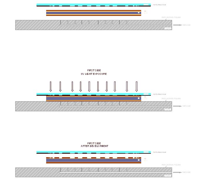
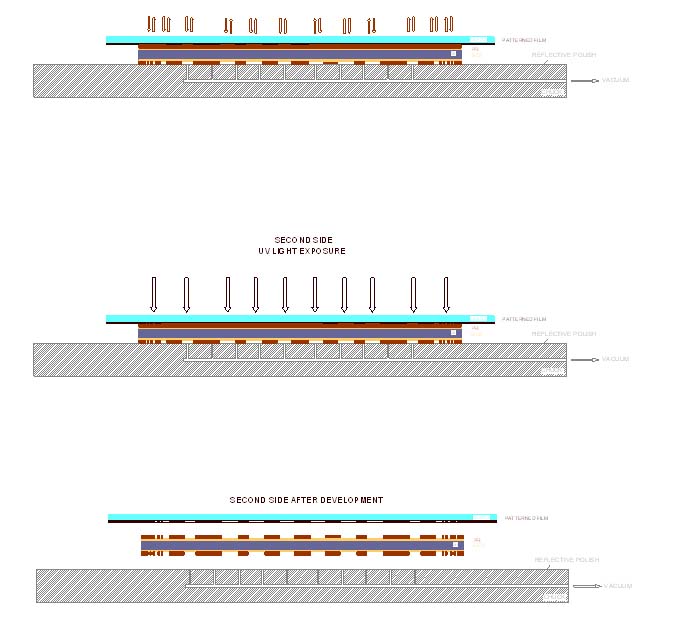
 The thin photoresist is
satisfactory for spin coating the wafers under
process as long as maximum etch depth is 4 microns or less. Beyond that
the thin photoresist does not cover the edges of the etched region well
even at slower spin speeds, and one has to resort to thicker (more
viscous) formulation of the PR. The thicker PRs are satisfactory down
to 20 to 25 micron etched steps, and beyond that they exhibit the same
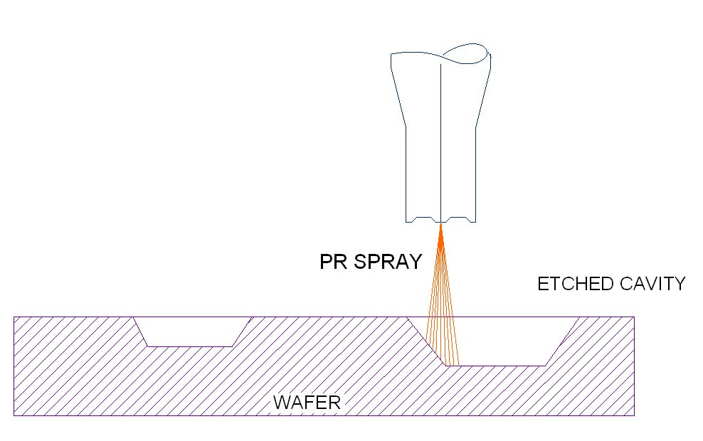
problems as the thin PRs at 4 microns. For etching deeper and etch
through wafers, a PR spaying technique (by an air brush as shown below)
is employed. This requires a much thinner formulation of the PR. As the
PR spray hits the uneven etched surfaces of the slowly spinning wafer,
it quickly dries up without giving the PR to run down and flood the
etched channels.
The thin photoresist is
satisfactory for spin coating the wafers under
process as long as maximum etch depth is 4 microns or less. Beyond that
the thin photoresist does not cover the edges of the etched region well
even at slower spin speeds, and one has to resort to thicker (more
viscous) formulation of the PR. The thicker PRs are satisfactory down
to 20 to 25 micron etched steps, and beyond that they exhibit the same
problems as the thin PRs at 4 microns. For etching deeper and etch
through wafers, a PR spaying technique (by an air brush as shown below)
is employed. This requires a much thinner formulation of the PR. As the
PR spray hits the uneven etched surfaces of the slowly spinning wafer,
it quickly dries up without giving the PR to run down and flood the
etched channels.
