


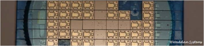

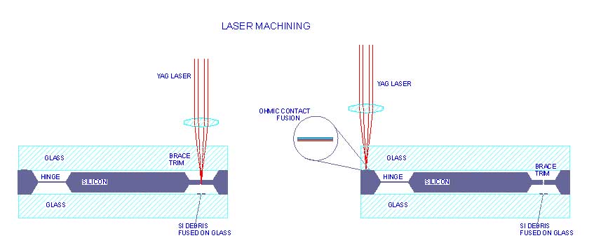
Laser assisted fabrication is one of the key processes in bulk micromachining of inertial navigation sensors. Generally, the sensing elements of navigation grade instruments are supported with very weak flexures so that very small changes acceleration or angular rate can affect the position of the sensing element, and thus, measure those changes. Devices are extremely hard to build with support flexures alone, because a slight jerk in handling the wafer can cause the sensing element to break off. Therefore, additional support braces are built around the sensing element for easy handling. Once the devices are fabricated and packaged between glass plates, the braces are trimmed off by laser, as shown in the left figure below. The laser beam is focused at the mid-plane of the brace. The beam is moved across the brace to burn off the silicon, the hot debris falls and fuses on the lower glass plate, as shown in the figure. The laser power is set high enough to melt the silicon and fuse to glass plate.
In its low power form, the laser is also used to make positive ohmic contact (welding of two metallic film surfaces bearing against each other), as shown in the right figure below. At microscopic level, a laser cut line is not as smooth as that made by etching along crystal planes. That's why it is difficult to form a complete micro device using laser machining alone.
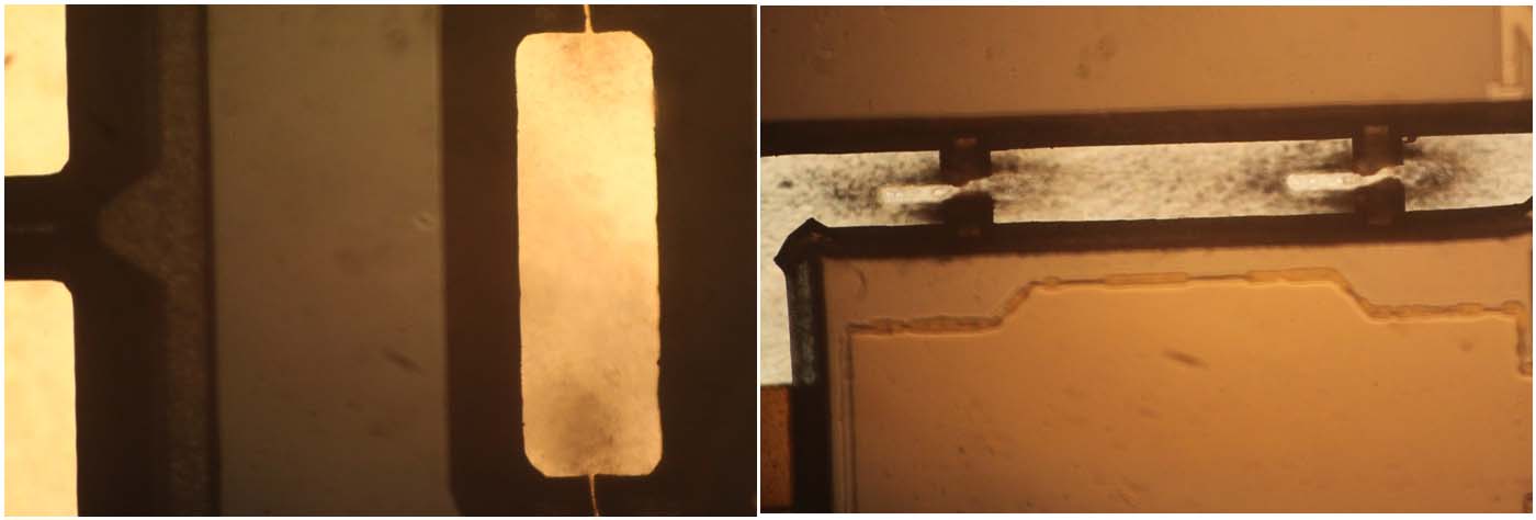
This photo shows actual cuts through silicon braces. The cross section of the braces is trapezoidal, and so the mid-section of the braces requires some extra passes of the laser to trim.
