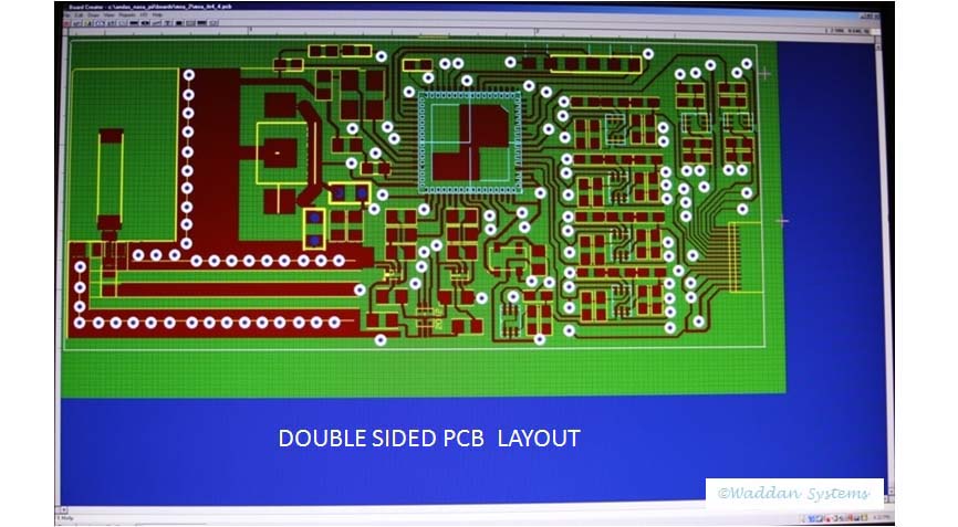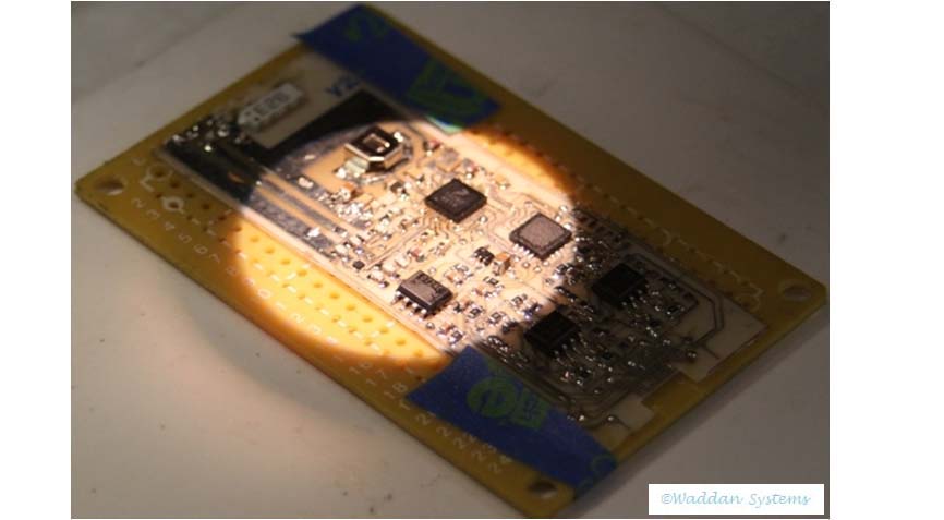


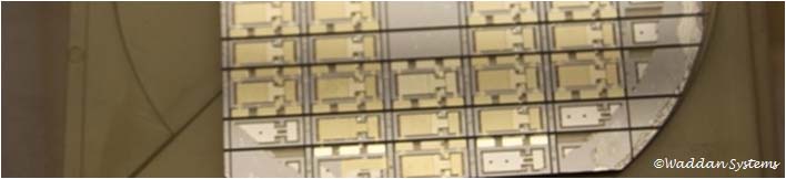

As everything else using electronics, with time the systems produced by Waddan have also shrunk in size. This trend required fabrication of small hybrid boards that included sensors and electronics. Any PCB of size less than 60mmX60mm can be easily adapted for processing through a 3” wafer fab tools. Therefore, an ultra-fineline PCB process was developed, that allowed copper line and feature separation as little as 1 mil. The thickness of copper layer on the fiberglass board is the limiting factor for obtaining narrower separations.
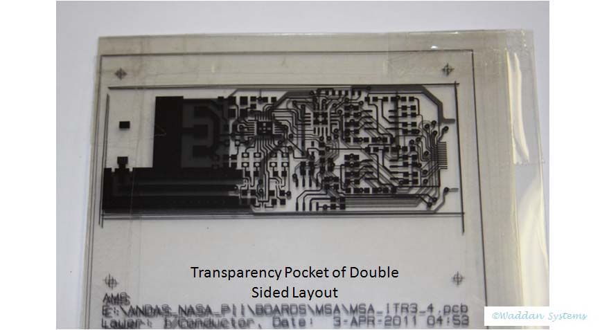
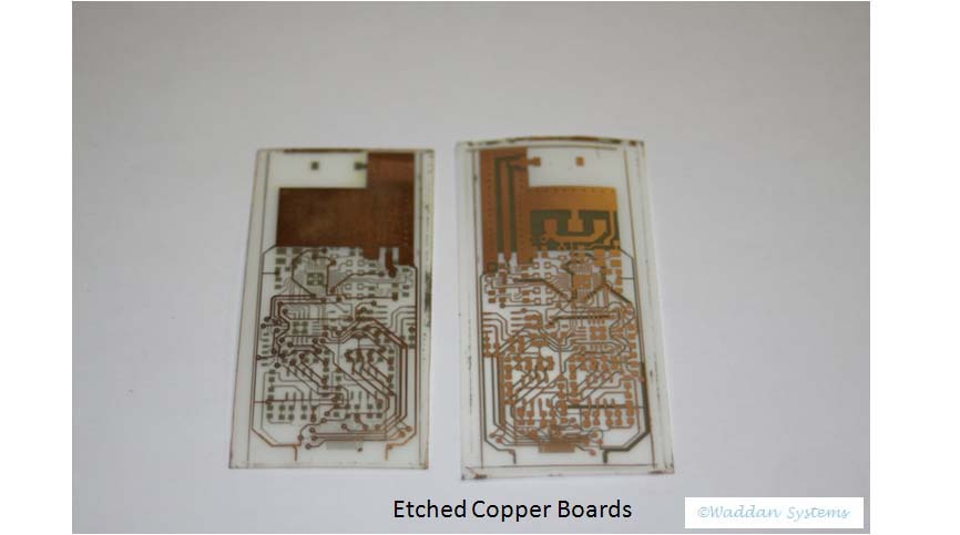
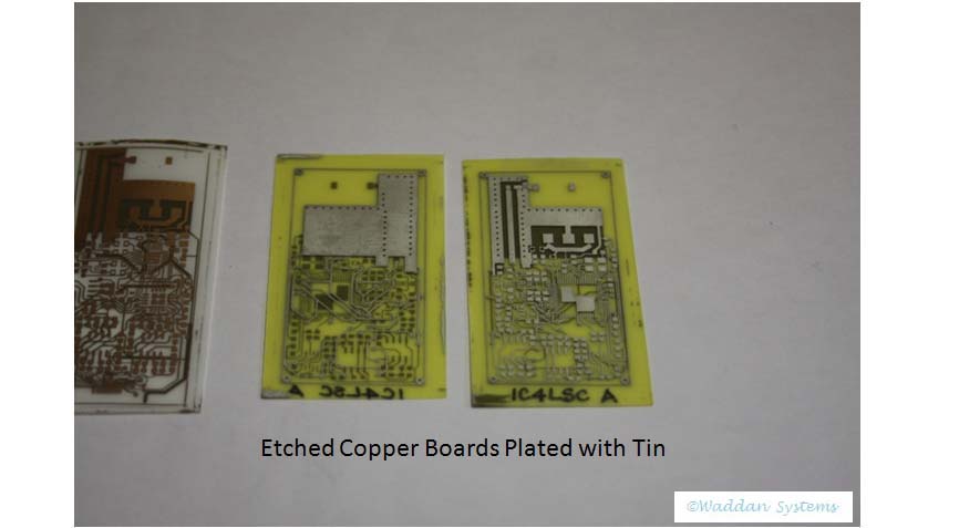
The general steps for fineline PCB processing are basically the same as those of wafer processing. The photolithography employs the same type of photoresist as the wafers.