


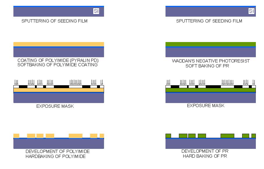
The familiar molding and casting employs a mold material to form a cavity with a desired shape. Molten metal is poured into the cavity through openings designed in the mold. Once the metal cools down, it forms a solid in the shape of the mold cavity. Then the molding material is stripped off leaving the solid. Micro-molding works somewhat in the same way. The mold is usually made in a photosensitive material like a photoresist, or polyimde or PMMA.
Waddan has settled on a negative photoresist approach for micromolding after trying out polyimide and PMMA initially in 1994-1995. The photoresist is mixed in-house in a safe-lite section of the Lab. The main component of the resist is EPON Resin SU-8 obtained from Shell Chemicals. It is dissolved in gamma-butyloracton (a solvant) to get the right viscosity, which, along with the spinner speed, ramp up and down and spin duration involved, essentially control the coating thickness . Coating thicknesses as high as 150 microns are obtained by a single coating step. The dissolving process employed includes a magnetic stirrer and a bottle shaker. The final component of the mix is a photoinitiator. A single step molding process is illustrated in the following diagram:


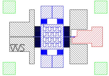
The diagrams show a single step mciromolding with
nickel. After electro-deposition the wafer is polished,
lapped, and annealed;a second step deposition can yield an intricate 3-D device.
Of course, the design has to be such that the photoresist from both steps
can be stripped.
On the right side a micro-molded accelerometer mounted on a header is shown. The pads on
glass base are wire bonded to the pin heads. The second photograph from the top shows the
construction of the accelerometer. The proof mass consists of a square plate with 16
rectangular openings made to reduce the mass. It is suspended by serpentine spring pairs
on the top and bottom. One of the springs is shown in the third photograph.
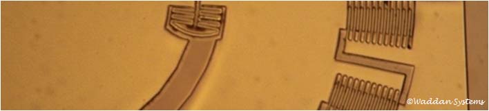
The electrostatic comb drives are located on the left and right of the device.
The tunnel diode pickoff consists of a arrow shaped tip facing a fixed flat surface.
Under normal operation, the proof mass is forced to the left until the tip reaches
in the tunneling gap region (between 5 to 15 Å from the flat surface). When the tip
is approximately 10 Å away from the flat, the accelerometer is at its null.
The sensitive axis of the device is along the direction of movement of the tip.
An acceleration input along this direction tends to displace the proof mass off its null.
A servo is used to develop electrostatic forces in the comb structures to counter the
inertial force to return the proof mass to its null. The electrostatic restoring force
is a directly proportional to the acceleration being sensed.
