


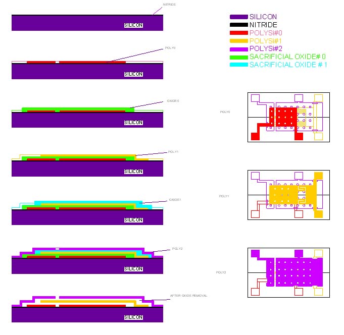
Surface micromachining uses deposition and etching of thin structural and sacrificial films to form the sensors. Waddan fabricates its surface machined devices incorporating simple microstructures like serpentine beams or diaphragms as well as complex structures like linkages, bridges or resonators on top of a nitride coated silicon substrate. The processing sequence for making a pendulous accelerometer is shown below. It employs 3 polysilicon films as micro-structural material, and 2 intermediate silicon dioxide films as sacrificial layers.
 .
.
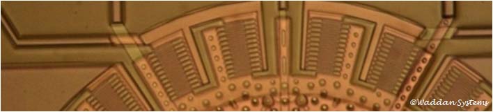
The processing begins with a single sided polished silicon wafer. Its polished surface is deposited with 600 nm thick silicon nitride film (shown in black) using our Tystar PECVD system at 250C. It serves as an isolation layer for the sensor signals. Next it is covered with first polysilicon film shown in red and labeled as PolySi#0. Its thickness is also 600 nm. A photolithography step removes unwanted PolySi#0 regions, and forms the bottom pickoff and forcer electrodes of the sensors. For charge balancing, the bottom electrodes have the same area as the top electrodes (see the circular cut outs). These electrodes are connected to two square pads of the device at the bottom. Next the entire surface is deposited with 2 micron thick sacrificial oxide (PSG). A photolithography step forms the gap regions between the bottom electrodes and the proof mass(this film is shown in green). The PolySi#1, shown in gold color, is deposited next. It is also 2 micron thick. A photolithography step forms the proof mass and the serpentine hinges . The large proofmass also has strategically placed holes for allowing the etching of green oxide underneath the proofmass. The proof mass is connected to the common square pads on the right hand side. Again a sacrificial layer of 2 micron thick PSG, is deposited and etched to form the gap between the proof mass and the top electrode. This layer is shown in cyan. The last film deposited is the PolySi#2 (shown in magenta). It is isolated from the proofmass and bottom electrode. It is also separated as pickoff and forcer--each connected to its corresponding square pad on the top. The photograph shown below is one of Waddan's surface micromachined pendulous accelerometer. In this device the proof mass is made much larger than the capacitive plate structures.
The main features of the surface micro-machining technology are the small microstructure dimensions and the convenence to integrate micromechanics and microelectronics on the same chip. By the use of LSI compatible batch processing, low cost microstructure fabrication can be achieved for high volume applications.
